The point here is: what happens if the tester is mistakenly connected to mains voltage?
A tentative approach would start by modeling the relevant parts of the circuitry that would be subjected to the negative swing of a mains cross-power event and by applying a constant voltage to the inputs.
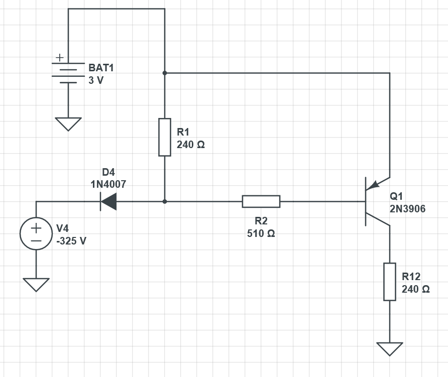
Power figures in case of no protection
As Leo mentions, R1 would need to dissipate over 400W in such event and clearly it’s not the only component that would be releasing the magic smoke.
The simplest type of modeling for the current limiting that comes to mind is to replace the voltage source with a current source set to -75mA (for a TBU-CAxxx-050-WH, datasheet page 2). This should simulate the peak current and voltage that the parts have to endure:
Power, voltages and ratings in the worst case scenario
Regarding voltage limits, the typical value is 150V-200V and it’s not of our concerns.
Power instead is relevant here, since we’re exceeding it.
A typical power rating for a 1206 resistor is 250mW. This value refers to the amount of power the component can safely dissipate into heat before reaching a damaging temperature and it also heavily depends on the component’s thermal resistance to the PCB and the ambient temperature (de-rating curves are also usually provided by the vendors).
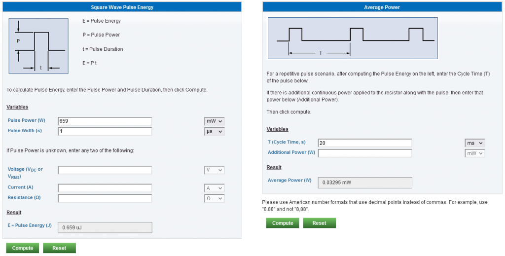
When it comes to pulsing energy into the resistor, in this case exceeding by 2,5 times the nominal amount, how much is too much?
In our case we’re going to observe a protection event per cycle, when the voltage goes below 0V and the threshold current is exceeded. This means that the event happens 50 times in a second, for a duration of a microsecond.
We can calculate the average power by using this tool (well, pen and paper would work as well!):
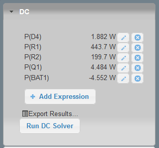
For simplicity, I’d consider a pulse of 659mW of 1uS, not considering the quiescent current upon which the TBU settles until it resets. This energy is pushed into R1 every 20ms, resulting in an average power of four orders of magnitude less than the maximum power rating of the resistor.
What if, as yngndrw asks, we use a TBU-CA085-100-WH, which triggers at 150mA?
R1’s peak power would go up to 2,5W, resulting in an average power of 0,125mW. Still chill 🙂
Q1 stress
For Q1 (actually in the circuit it’s a BC807) I hope it’s enough considering its relevant maximum ratings:
Measurement
Max rating
With TBU-CAXXX-050
With TBU-CAXXX-100
Vcb
-50V
1V
1,26V
Vce
-45V
-39mV
-37mV
Veb
-5V
1V
1,34V
Ic
-1A (pulsed, 1ms)
-12mA
-12mA
Ib
-200mA (pulsed, 1ms)
-22mA
-46mA
Ptot
250mW (safest)
24mW
60mW
Therefore it seems that even the BJT might be able to comfortably survive with either TBU.
A couple of weeks ago, YouTube suggested me this video:
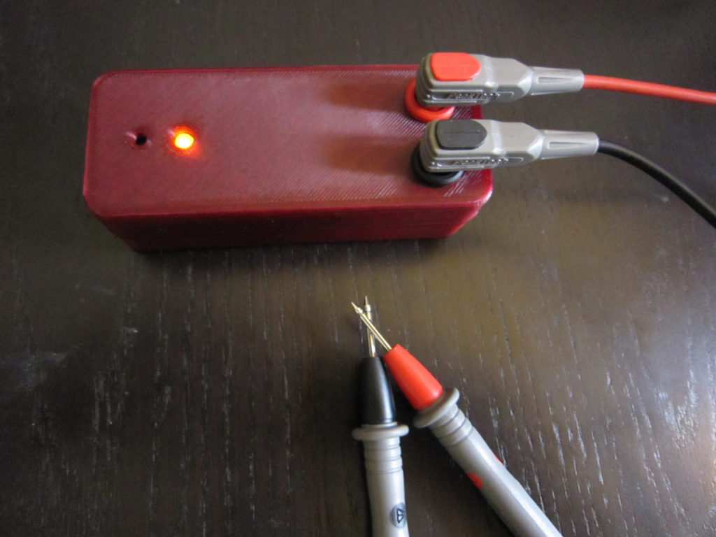
Leo’s bag of tricks take on continuity test
I found myself quickly enamored by the idea, since I believe that a tool must be fun to use. And by fun I mean no double thoughts about its reliability, and that it should be easy and predictable.
The video has a great progression: the goals are clearly outlined along with the steps to satisfy all the requirements.
I decided to give it a try and to realize it and document the process here. Here you won’t find the way the device works, since Leo has done a great job already on his video.
A follow-up article has been written to focus on the protection offered by the TBU and it can be found here.
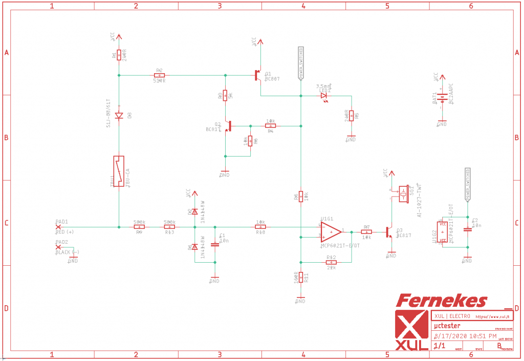
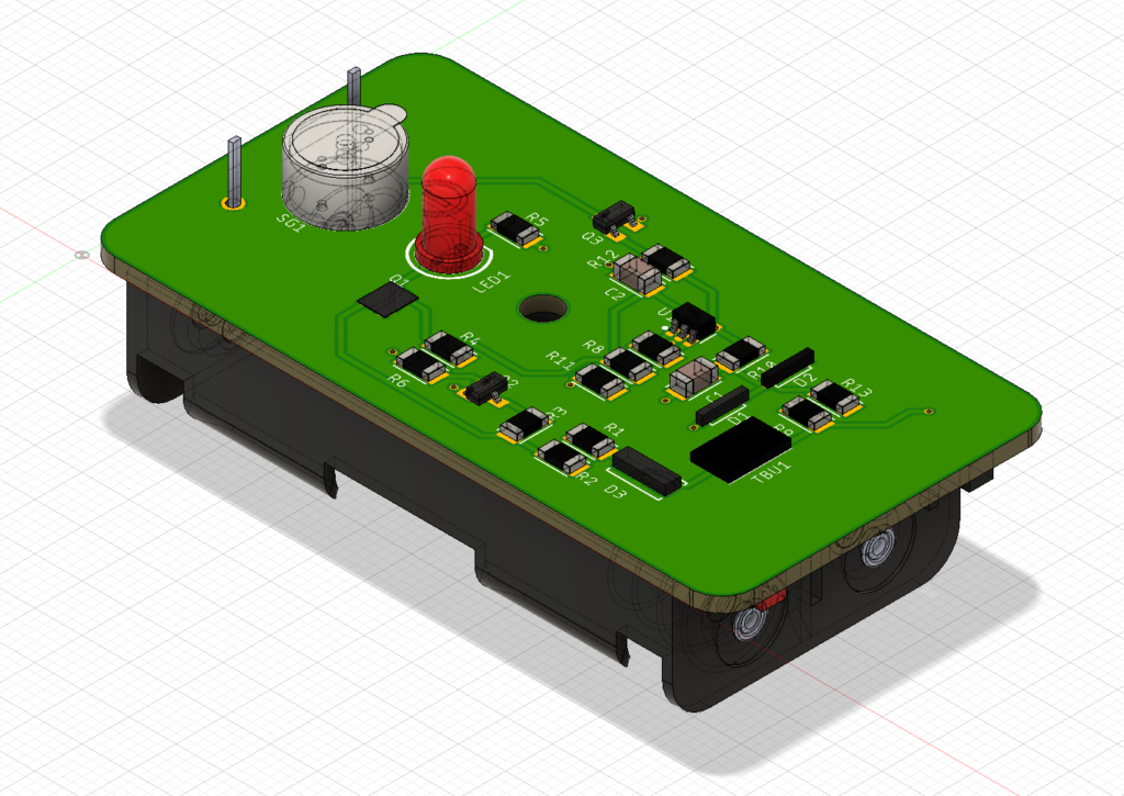
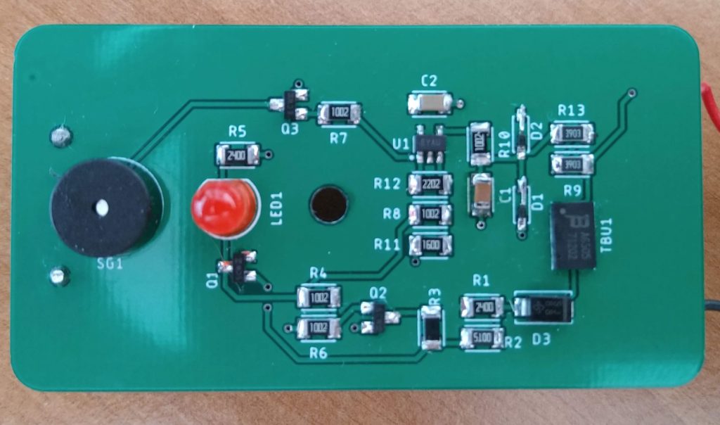
Schematics
Leo kindly provides a PDF of the schematics of the design which I captured as-is into EagleCAD. The only minor changes I did were to employ SMT-only packages, a single-opamp (MCP6021 in lieu of the MCP6022), and BC-series BJTs, just because I had these parts at hand.
Revision B of the schematics
A rough breakdown of the time spent on the schematics:
20% capturing
40% searching and checking options for some special parts (buzzer, batteries holder)
40% modeling new parts
In spite of its simplicity and that the design was given on a silver plate, I managed to commit a mistake by connecting the power rail of the opamp to VCC, instead of Q1’s collector (the main soft switch).
Obviously I realized it only after ordering the PCB for revision A 🙂
Debouncey
There’s one thing worth mentioning, which is the role of C1.
In the way it’s set up, it forms a low-pass filter to the input, with an approximate cutoff frequency of 15Hz. This prevents the opamp to rapidly strobe the buzzer with an annoying screechy sound when the input bounces around the triggering threshold.
Its value is a tradeoff between reaction times (the beep should come fast) and false re/triggering (so not that fast). I guess there are more convoluted ways to avoid the compromise (signalling as soon as possible and latch for a couple of milliseconds).
I’m not sure how Fluke multimeters continuity tests manage to have that amazingly fast reaction times with a perfect rejection to bounces and I guess that if there’s any possible way to improve this design might lay upon this feature.
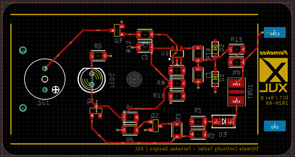
Routing
Routing the board was really easy, given the low components count and ample surface.
PCB revision B, ratsnest ripped up
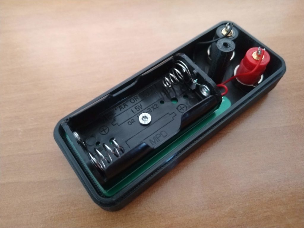
The size of the PCB has mainly been dictated by the batteries holder, which I decided to be soldered to the PCB instead of having it connected by lead wires.
Once the routing was done, I branched off a bit before committing its final dimensions and locations, and pushed the board to Fusion360.
Gerber view of the top layer of the PCB
Thinking ahead about an enclosure
At the moment (August 2020) an Autocad Eagle subscription entitles to Fusion360. I’m not sure what will be the future of these two products, since I have the impression Autocad will slowly phase out Eagle as a standalone product, focusing on its full integration into Fusion360.
Pushing to Fusion from Eagle is a very simple process and given that the components in use have associated 3d models, the result is quite spectacular:
The PCB as it looks when imported from Eagle to Fusion360
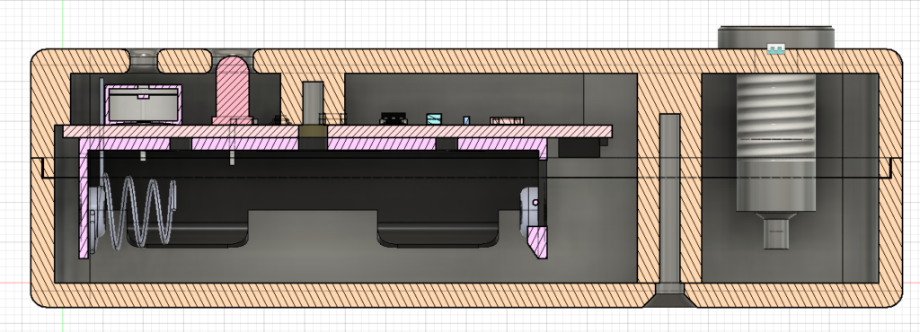
Once imported to Fusion, I was able to consider clearances, components locations, mounting options and how to expose the pads for the banana connectors in respect to an early idea of an enclosure.
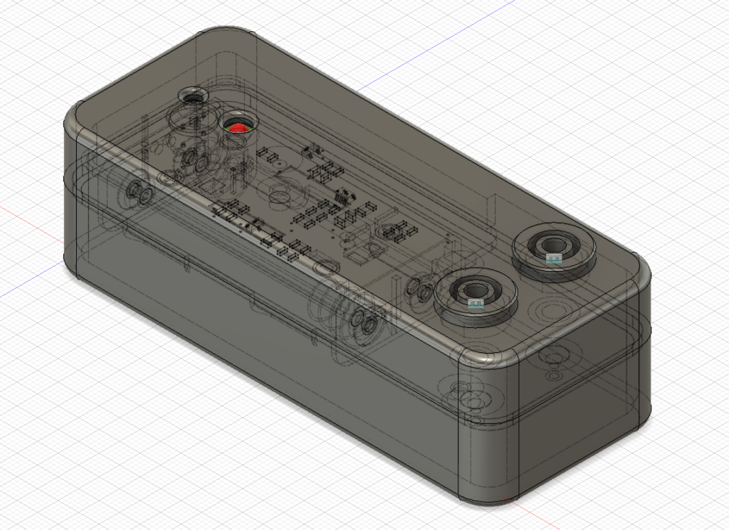
The final model of the enclosure
Far from being savvy about modeling, I chose an easy two-parts shell, which can be explored here.
By adding the connectors I was able to define the final sizes of the enclosure.
Position of the LED
PCB mounting standoff in view
Other relevant features:
LED and buzzer position (plus projected holes)
PCB standoff and mounting point
Shells coupling
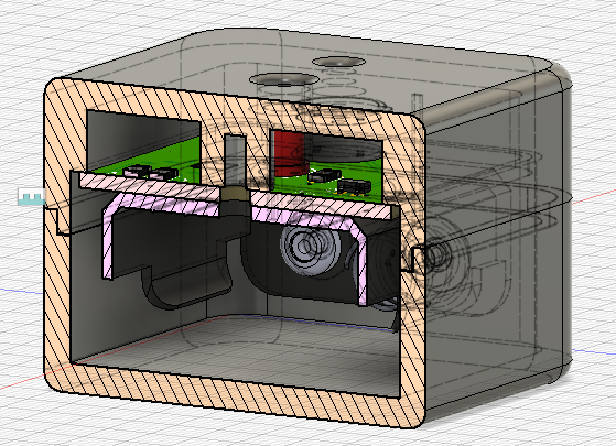
LED and buzzer
These two components are exposed to the outside via holes.
On the first revision of the enclosure I modeled the buzzer hole a tad too little (1mm diameter). The buzzer is still audible but it’s quite muffled. The latest version has a bigger hole with a gentle fillet around both sides.
The LED could had been a bit more exposed, but I had to compromise with the length of the screw.
PCB standoff and mounting
The PCB lays on a rim which offers a lot of clearance and it’s firmly held in place by a standoff pillar and a 10mm self-driving screw.
The LED functions as registration point, keeping the PCB from rotating on the pillar’s axis.
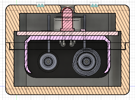
Shell coupling
I opted for a an alignment edge (is there a better term for it?) plus a single screw. The two work marvelously together, even if the screw is offset from the center.
Side section analysis: alignment edge and pillar
As visible from the picture, the edge prevents rotation or shear, while the pillar couples the two parts together.
Initially I considered the option of embedding a nut or a threaded insert into the pillar. Having zero experience on materials and required clearances, I decided to go easy and to use the same hole pattern (and screw) planned to hold the PCB in place. Servicing the batteries should be done only once every lifetime anyway 🙂
The screws I used are 8x3mm self tapping, 90deg countersink, flat head.
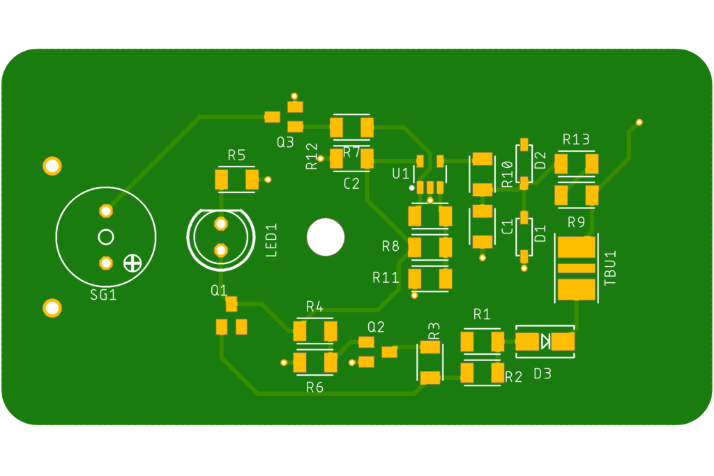
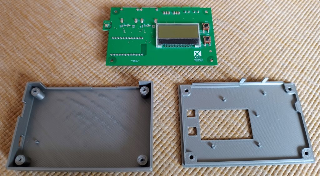
PCB assembly
I chose 1206 passives, given the low parts count and plenty of surface to waste.
The PCB (rev A) assembled
I had to solder the TBU with hot air, everything else required a mid-size soldering tip.
The two 1n4148 I had available were in a different package (SOD323 instead of SOD123) so I had to extend one side. The 390k resistors on the picture for R9/R13 as well are a temporary replacement of the 500k ones.
3D Printing
The enclosure has been sliced up with PrusaSlicer and printed with a Prusa MK3.
Timelapse of the first print
The two shells mated perfectly and the only thing I had to do was to de-burr the edges of the banana connectors (most likely they’ve got tapered).
As mentioned above, the only pending modification for a “final” print, would be the size of the buzzer’s port.
Testing and using it
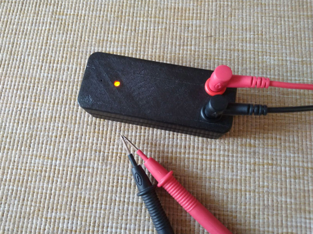
I realized quite quickly that I was used to continuity testers with a high resistance threshold (Leo shows how a Fluke 87V beeps already at 50Ohm). By connecting a pair of probe leads I noticed that the tester beeps steadily with a firm contact of the two, but it gets flashy even by just sliding the two contacts together.
I was taken aback, but it’s actually true that imperfections of the surface and contaminants can cause sudden jumps in the conductive path. Most of the test leads are pointy and they’re able to penetrate dirt and sometime oxide layers.
I agree with Leo that real continuity is definitely not 50Ohm, but I haven’t had the chance for an extensive field test to prove that 5Ohm is an ideal threshold.
The nifty feature about the LED and buzzer being driven by two different thresholds is that one can still distinguish between low impedance and continuity and this accounts also for diode testing.
So, I’m sure I’m going to love this tool. It fits snugly in the hand and allows to clamp one of the leads along, even though it might be a nifty feature to add a magnet and/or a clip to the box.
Credits
Concept, idea, design is Leo’s, whom I thank for the instructional video and sharing. Check his great YouTube channel here.
Thanks for the support for the 3d printing to Johannes H.
And thanks to Uli F. for the modeling tips.
Files and downloads
Eagle Schematics, board files, gerber and BOM can be found here
It happens more or less regularly that I find myself in the need for a temperature logger. When I do, I always regret not having something more practical than proto boards, sensors and the usual big question mark on how to gather and then analyze data.
In spite of the fact that I know that there are already solutions out there, definitely more mature than any weekend-job attempt that might never see a revision B, I find “reinventing the wheel” quite charming for learning and refining design and problem-solving processes.
I ended up with a device that could be used for applications such as:
Long term temperature and environmental data logging
Datacenter temperature and humidity monitoring
Reflow controller
Air quality logger
Oven calibration (well.. cakes need precision)
Sous-vide controller
Ramen broth controller
Even though the primary purpose of the project was, at the end, to write this article and condensing the whole experience into a shareable medium.
The big picture
I started from a set of requirements for this wannabe device:
support for two thermocouples
optional support for DS1820 1-wire sensors
onboard environmental sensor (at least temperature and humidity)
onboard user interface
flexible connectivity options: network (ethernet or WiFi) and serial
output for relays or general purpose actuators, at least 2 channels
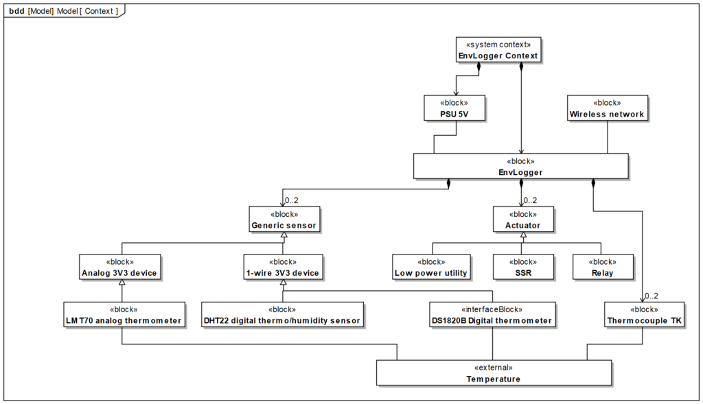
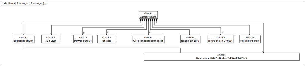
Then I sketched a BDD diagram of the context, describing the interaction between device and the great outdoors.
BDD of the operating context for the device
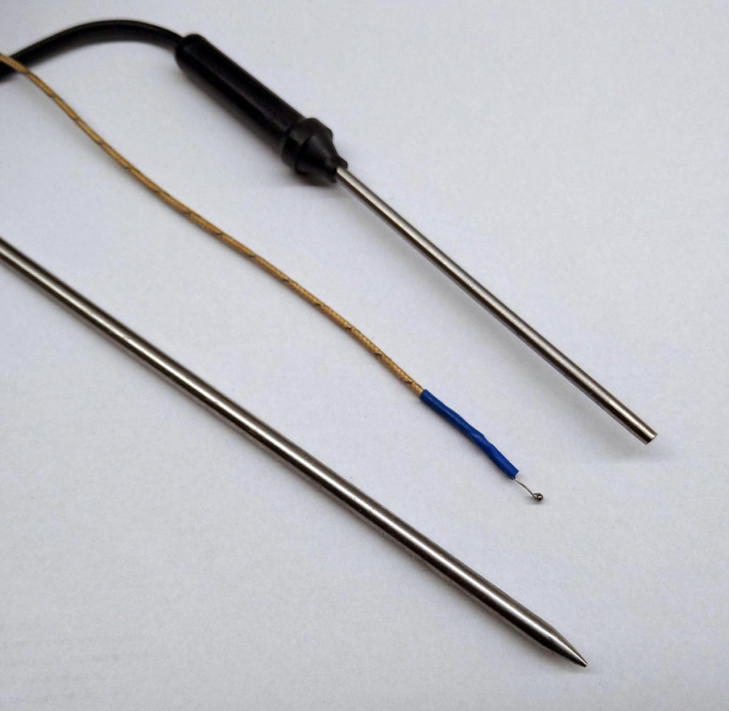
Thermocouples
My toolset for temperature reading:
an IR thermometer to sample quickly and on broad, non-shiny measuring targets
a NWIR camera to sample heat propagation and distribution on a system
Thermocouples are cheap, fast, easy to obtain and to bind to the target. Since universe is balanced, there’s a con, which is precision. For almost all my task though, ±1C isn’t a big deal.
RTDs are thermocouples’ competitors and increasingly used in industry. They’re more linear, more precise, more slow, and more expensive. But in spite thermocouples to come in many varieties (with balanced pros and cons) and their nasty non-linearities, there are plenty of specialized chips that don’t need anything else than an I2C bus and a proper connection to the cold junction.
These sensors are very easy to integrate since they require only one data pin (Dallas/Maxim 1-wire), plus ground and eventually VCC (unless a special mode called parasite-power is used) and there are libraries for arduino and mbed.
Other types of sensors that require only three pins (including power) are the notorious DHT11 or DHT22 ambient temperature / humidity sensors.
And for another category, this time analog, it is worth mentioning TI LMT70 and TMP36, analog sensors that operates also with 3V3. The more popular LM35 doesn’t work at 3V3.
Actuators
Splatting a couple of MOSFETs as output driver is a no-brainer. Since this unit could be used as a PID controller, having an output stage might come in handy.
Then, let’s add two open-drain outputs.
Connectivity
Ethernet is the only protocol stack that has never let me down.
It has also the advantage, when dealing with low-power devices, to be able to source power via PoE and with chips like WizNet W5500, it’s rather easy to integrate.
The reason why I chose WiFi for this project lays on two relevant points:
I thought about using Particle’s products, which are heavily wireless-connectivity oriented
In my typical use case, when ethernet is available, so does WiFi
The reason for the first one is the answer to “what can I do to finally use this dusty protoboard?”. Jokes besides, I like the quality of Particle’s workflow and documentation: they offer a wide variety of options for handling devices and communicating with them. Including a working OTA concept, which is a crucial point for a device that is not directly connected to any host (that can easily push firmware updates to it).
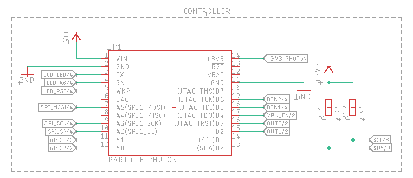
Particle offers development kits and compact modules, such as the P0 (this one in particular for the barest WiFi connectivity).
I had to relinquish my crave for minimalism (or maybe I did not) and extra soldering challenges and opted to integrate directly the dev kit onto the board.
So, WiFi, let’s see if I can trust you.
One layer below
So far I described the process to evaluate requirements starting from the outside world’s context, with some digressions to the actual components that might be used to achieve such interfacing.
Now I’d go one step further, into the composition of the board itself.
BDD of the innards
Display
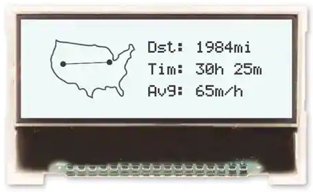
I like OLED displays, in particular the tiny 128×32 like this one. But, taken by a need for seeing the display directly attached to the board instead of being mounted on an intermediate carrier, I searched what Digikey had to offer and, to my disappointment, I didn’t find anything suitable.
The selected LCD. The US map is definitely photoshopped.
I ended up choosing a pretty standard FSTN LCD, backlit with white LEDs, 128×32 pixels: Newhaven NHD-C12832A1Z-FSW-FBW-3V3. SPI interface, 3V3.
The reason for the SPI interface was a lazy choice for speed. I didn’t even bother checking whether I could do everything with one single I2C bus since I had the interface available.
Environmental sensor
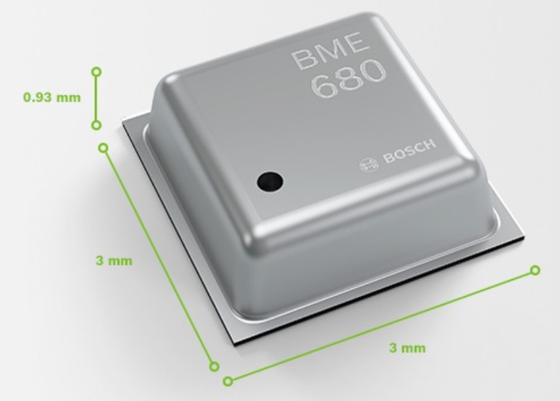
Ehm, courtesy of Bosch
For a recent project it happened that I needed to keep constant track of the relative humidity in a room. I’m a fan of Bosch-Sensortec products and the BME680 was a perfect fit (besides its cost). It’s a little marvel: reliable and complete, offering sensing for:
The sensor speaks both I2C and SPI. I chose to use the former since I didn’t need bandwidth and because I decided that all the onboard sensors could had been suited conveniently by a single bus.
Thermocouple EMF converter
In two words, thermocouples generate an electromotive force which depends on the temperature difference between their two ends (hot and cold/reference junction). Wikipedia can shed a better light on the matter.
The whole point of measuring a temperature using a thermocouple, then, is to:
Sample the detected EMF into a known quantity V
Measure the temperature of the cold/reference junction Tref
Apply some type-related adjustments E(T) (each type has its own characteristic function)
The result is E(Tsense) = V + E(Tref)
So, instead of doing all this, let’s find the right chip!
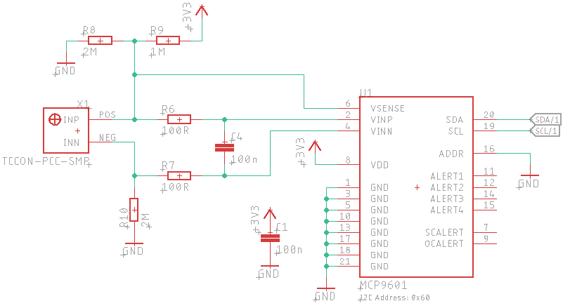
I don’t remember why I haven’t trusted Adafruit’s options for a thermocouple converter (such as the Maxim-Integrated MAX31855, which I’ve already used in the past) and ended up selecting the Microchip MCP9601, another pretty nice (and again, expensive) chip.
Such decision had probably to do with some kind of masochistic will to create an Eagle CAD part and to write a driver for it too (there’s nothing better to understand an ASIC than to talk to it).
Integration of the MCP9601 thermocouple EMF converter
The circuit above shows the way the chip has been integrated:
R6, R7, C4 form a low-pass filter
R8, R9, R10 set up the open circuit detection
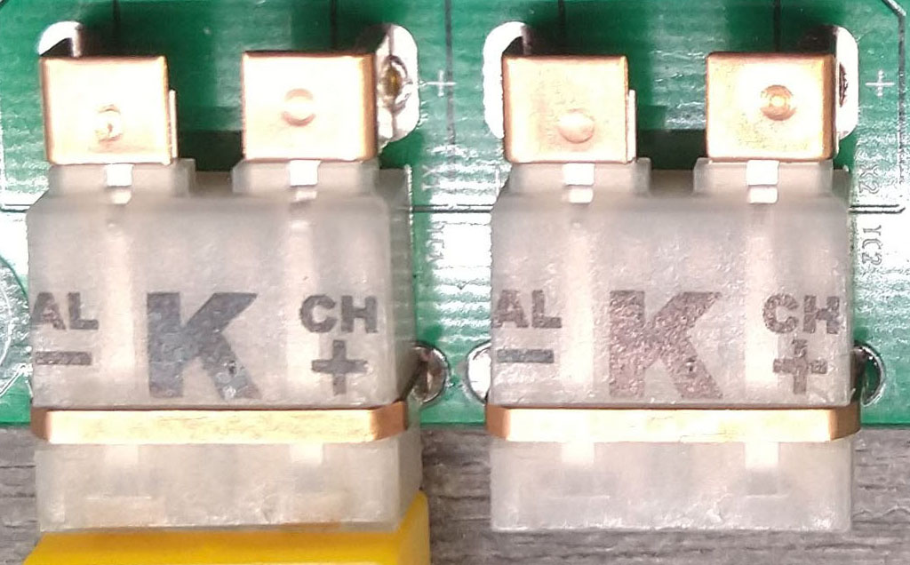
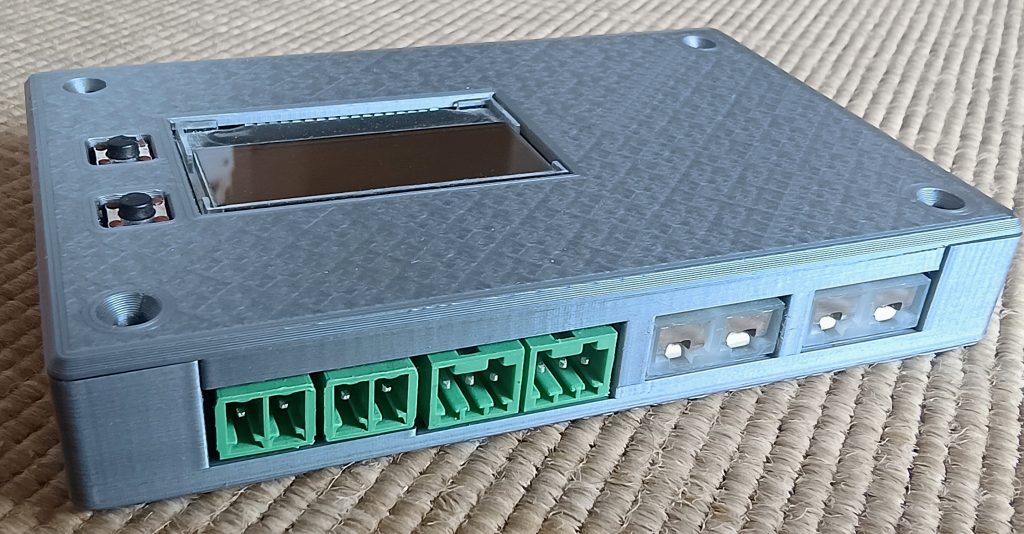
Thermocouples termination connectors
I had some hate for the standard “miniature” connectors for thermocouples. Probably because I have always had the bad luck to use loose receptacles. It’s not uncommon that a logging session had been jeopardized by a flaky connection, but I aimed to integrate them nevertheless in lieu of a brutal screw terminal.
Since these connectors act as terminator for the cold/reference junction, it’s quite vital that they have a minimal thermal resistance to the component that measures its temperature.
Searching for a proper option in Digikey didn’t yield much, besides a product distributed by Sparkfun, that gave me a new hopes for this connectors type. The one I ended up using is the Omega PCC-SMP.
These connectors are robust, they offer a copper bridge to prevent tilting and they have a satisfying (herculean) insertion force.
Type-K thermocouples are made of Chromel and Alumel (two Nickel-rich alloys) and their relative connectors (both plug and receptacles) are made of the same materials. The receptacles contact terminals end in copper stubs (as it can be seen in the picture above), soldered then to the board. That’s the so-called cold/reference junction and that’s the point that should be measured to get a reference readout.
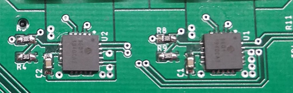
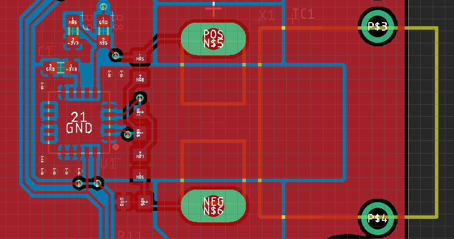
PCB layout showing how MCP9601 and receptacle are connected
As shown above and by trying as much as possible to follow the guidelines described in the MCP9601 datasheet, chip and connector are placed in a way that tries to keep them close to each other, sharing copper planes to reduce their mutual thermal resistance (as described below, this doesn’t seem the case).
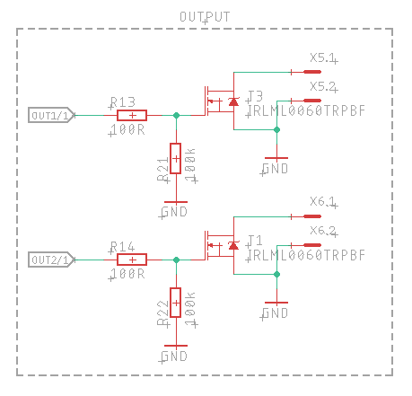
Power drivers
For the output drivers I chose two general-purpose 60V 116mOhm N-MOSFETs, namely the Infineon IRLML0060TRPBF and set them up in an open-drain configuration.
General purpose open-drain outputs
For the newbies (I’m among them, let me repeat the mantra): the series resistances R13, R14 limit the peak current that the gate tends to sink/source due to its capacitance during level changes, while the ones to ground (R21, R22) ensure that the gate charge is sunk when the OUT1/2 driving pins switch to high impedance, keeping the MOSFET at a determined (off) state.
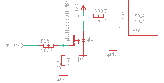
LCD backlight driver
The exact same setup has been also used for the backlight LEDs of the LCD.
Buttons and UI concept
Two buttons seemed to be enough for a minimal user interface. The reality is that even now I still don’t know for sure since I haven’t defined any specific user interaction model nor I have a storyboard.
Due to the potential flexibility of the device, I’m not sure if there will be only one firmware “to rule them all”, as opposed to the more probable approach where the firmware is prepared ad hoc and used for a specific scenario.
I’m not even that sure I’ll ever use them too..
Anyway the buttons are simple tactile SMD ones, nothing magic about them.
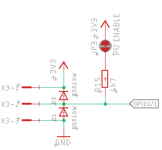
Extra inputs / GPIO
Since I’m using the DS1820 quite often and supporting them is no effort, I added two inputs, served by two three-pins Phoenix connectors that conveniently deliver power to the sensors too.
Auxiliary input (well, also output) stage
1-wire communication on these inputs can be enabled by shorting the solder bridge.
Power
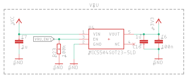
The 3V3 voltage regulator
I didn’t want to use the Photon’s LDO VRU (the datasheet indicates a maximum allowance of 100mA), therefore I added a Microchip MIC5504 300mA LDO. The Photon is able to shutdown the power to the external devices via its enable pin.
Schematics and PCB layout
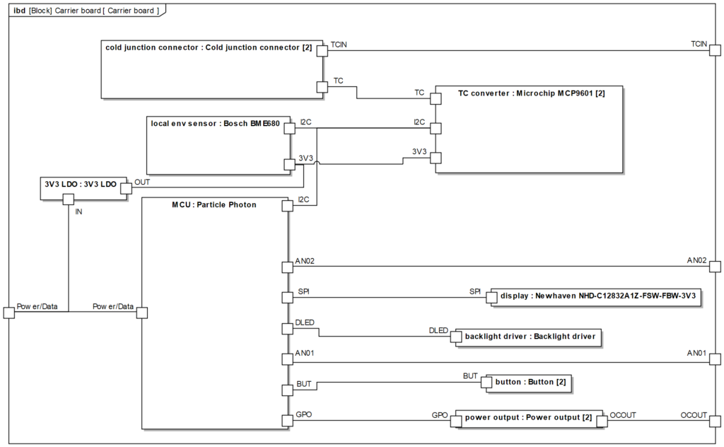
IBD of the components
One of the longest task I went thru was to create the missing components in Eagle CAD.
The most complicated unit was, surprisingly, the LCD. The dimensional drawings provided on the datasheet are lacking vital information, plus being plain wrong (the second drawing shows details of another unit). Since I was running the design in an lazy/express-high-risk-weekend mode, I didn’t have the unit at hand before designing the part (not a good practice, true).
But, then I found this repo, which I used to cross-check the footprint (kudos to the author).
The schematics didn’t pose any challenge, it was mostly following guidelines described by the datasheets and a bit of pins assignation scrambling (more about this later).
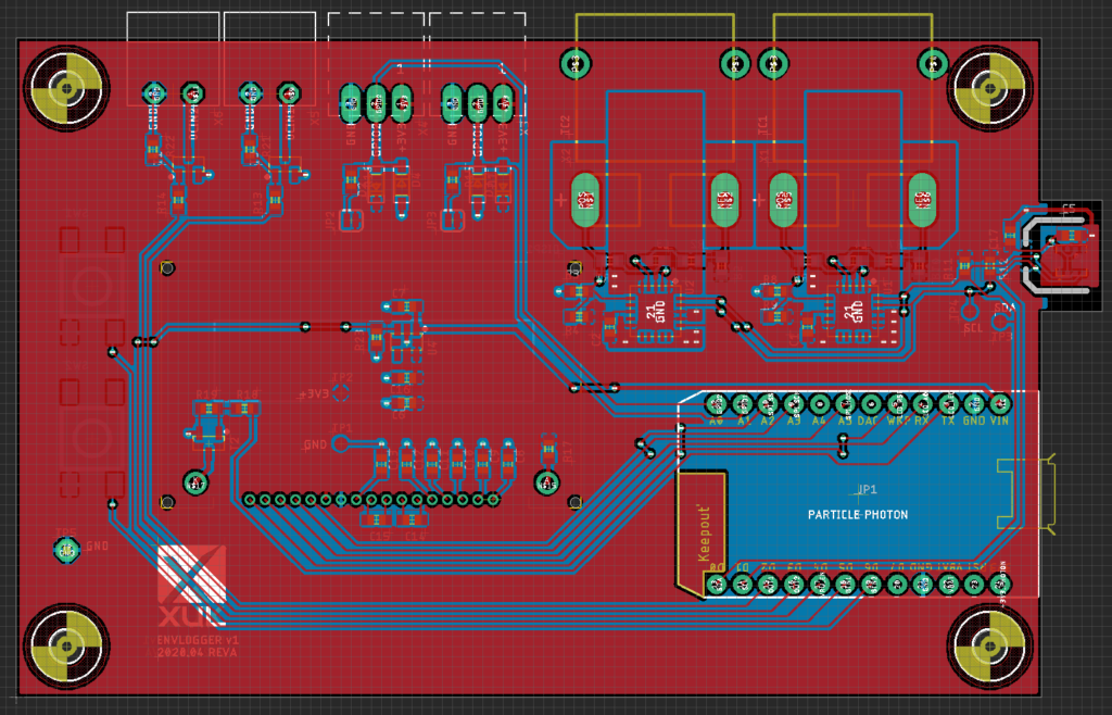
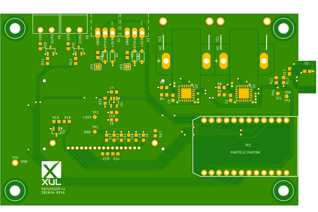
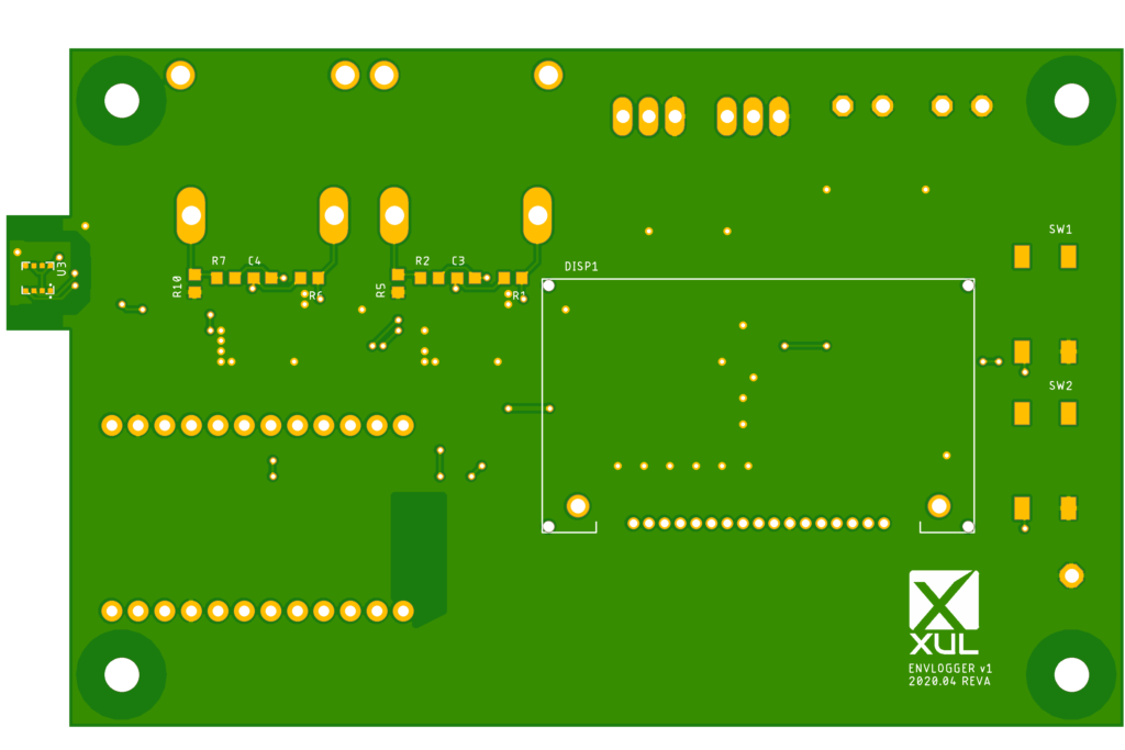
Revision A PCB layout
PCB layout
The PCB layout wasn’t complicated either. I followed some constraints such as:
MCP9601 as close as possible to the connectors
3V3 VRU far from BME680 and MCP9601
Photon on the edge to facilitate the USB connection
BME680 as (thermally) isolated and exposed as possible
Buttons on the right side of the LCD
Revision A ended up being a 2-layers standard 1.66mm FR4, 107mm x 65mm (yeah, those 7mm hurt), routed primarily on a metric grid.
Top viewBottom view
The only relevant note is the funky shape due to the BME680 peering out. I just imagined an enclosure and that little tongue coming out of it. Similarly to the UI, this is another part where I should had invested a bit more, since Fusion360 was just invoking the Gods to be used.
Anyway, it’s not visible on the gerber rendered files, but the BME680 is trenched out to increase thermal insulation with the rest of the board.
Ordering
I ordered the PCB from JLCPCB (not sponsoring). One week and the package was in my greasy hands, for a total 24,77€ (5 PCBs). I have been using their service quite often and I’ve never been disappointed and this price is just insane (considering that the cost of the service, excluding shipment, was 5,90€ and just because I exceeded the maximum size of the cheapest option by 7mm).
Soldering
I have the impression I badly wanted to prove my viper skills here as well, choosing 0603 passives and deciding that the BME680 had to be mounted to the bottom layer.
The reasons for both:
Soldering 1206 components is piece of cake and a pleasant experience, but I started to stock 0603 passives since I use them quite often
Bottom is supposed to be the side facing the user (the UI is there) so I imagined that exposing the sensor meant it to be on this side, having also the advantage to be on the opposite side of the active components
I didn’t reflow the whole PCB, since I wanted to practice air soldering for QFN and LGA. I was a bit worried to damage the BME680 without a proper soldering profile, but apparently it worked out pretty good, with just one soldering attempt per chip.
But reflow makes hell of a sense and having all the critical components on one side only would help a lot.
Issues
Well, first of all let’s say that the first (and only..) assembled board worked out completely fine without any trace-cutting and/or jumper wire.
But there’s an annoying but foreseeable issue I didn’t take into account: the Photon board produces a relatively high amount of heat when operational. And this, so to say, is a problem.
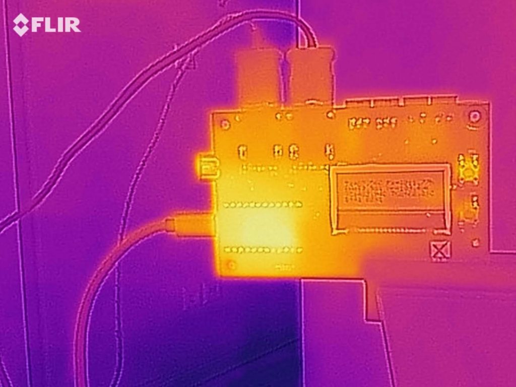
The Photon runs hot (and the BME680 too, with the VOC sampling enabled)
Relatively to the BME680, I was taken aback by the rapid (~1 minute) ~+5C increase measured after powering up the device, but the picture above (where the VOC sampling was active) and the one below (where it wasn’t) cleared out the fact that the reason was the device’s self-heating. The device has an internal heater for the VOC sensor and it’s more than obvious that triggering it every second definitely contributes to a substantial increase of the temperature of the device itself.
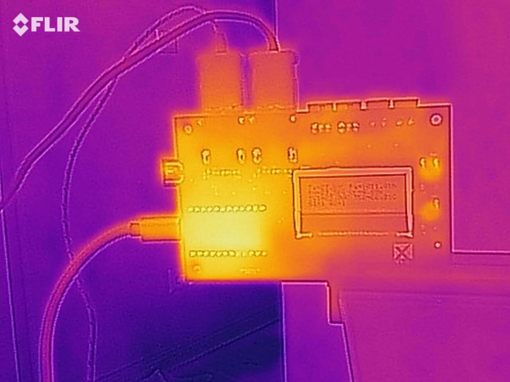
BME680 with the VOC sampling disabled
On the other hand, it shouldn’t be a big deal for the MCP9601s, since the whole point of measuring the cold junction is to establish a reference point, right?
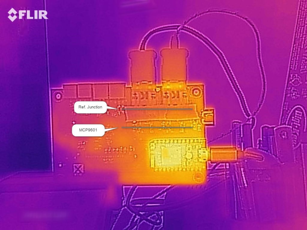
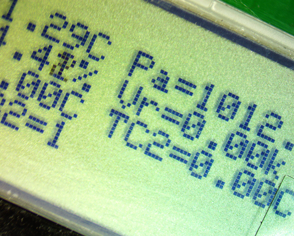
Yeah, sort of: there’s a slight temperature difference between the MCP9601s and the reference junctions (as shown in the picture below).
Anyway, the thermocouples disagree with the BME680 by just an average of 0,8C.
The temperature difference between the MCP9601s (lower line) and reference junctions (upper line) is about 0,5C. The copper terminals are covered with tape to avoid IR reflections (that are visible from the upper collars of the TC connectors)
Probably an enclosure might help to equalize the heat. The orientation of the device also changes a lot the boundary conditions. Or maybe running the MCU and WiFi at their lowest power mode possible. Or maybe just redesigning the board? 🙂
Almost all pins are in use. The assignation logic here was:
SPI1 to the LCD
I2C for the sensors
Backlight and outputs must be on PWM-capable pins (I love the fade-in of the backlight when the unit starts)
More information about the Photon can be found on its online datasheet.
Testing
The first bits of code I write are usually those that help to track issues on the design. Basically testing the functionality of each individual component placed on the board.
But a short digression in how the Particle units handle their operations.
Cloud particles and system modes
One interesting aspect of the devices offered by Particle is the incredible baseline equipment they’re delivered with to join the cyberspace. Devices can be maintained from a centralized console, firmware updates can be delivered OTA, events can be streamed and more.
Since the easiest starting point is to use their web IDE, I gave it a go.
particle.io Web IDE
I had been using a bit the IDE in the past for a couple of blinky tests, but this time I hit quite immediately its limits. Adding files is doable but not a snappy experience and it happened twice that for a classic “endless for loop” I ended up with a device that was unable to join the cloud again. No cloud, no OTA, no OTA no fix.
In spite of the fact that it’s quite easy to put the device in DFU and reflash a working nothingness, it shifts the attention from the Web IDE to a local setup (using the CLI tools), therefore I decided to switch to the local domain altogether using the Desktop IDE, based on VSCode.
I must admit I don’t like VSCode much. After hating Eclipse for years, it has become my best friend. Even if using Eclipse with Particle devices is somehow documented, the only guide I could find describes how to use it for SWD/JTAG debugging. I simply didn’t try.
(besides, I’m a vim-er, not an emacs-er, if anybody might ever be curious).
But then the next thing I’ve done was to switch the Photon to MANUAL system mode (no WiFi, no cloud by default). The cloud functionality is cool, but it slows down brutally the flash/test cycles.
Testing the components
Needless to say that the very first thing I forgot is that without enabling the LDO VRU there was no juice for anybody. It’s a classic bad feeling when a short on VCC is going to ruin your day, but instead:
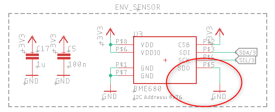
The BME680 is configured for I2C address 0x76 (SDO is connected to GND):
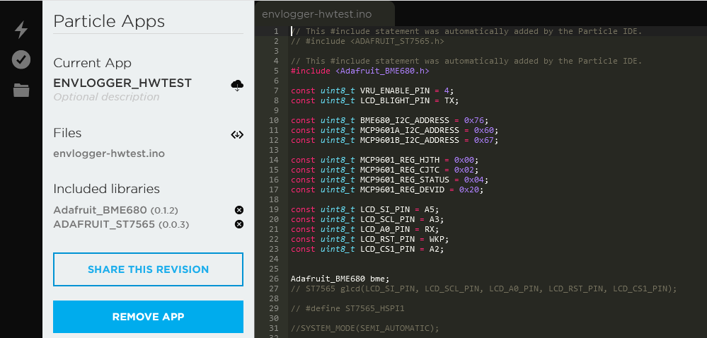
Testing the BME680 was the first, easiest task, since Adafruit provides a library (ported to Particle):
> particle library search BME680
particle-cli v2.5.0
Found 2 libraries matching BME680
Adafruit_BME680 0.1.2 12607 Library for running Adafruit BME680 on Particle Photon via I2C
Adafruit_Jib_BME680 1.0.8 202 Library for running Adafruit BME680 on Particle Photon via I2C. Possibility to adjust Gas Sensor.
The gist of the test code is this:
void bme680_update()
{
    if (!bme.performReading()) {
        Serial.println("BME680: Failed to perform reading");
        return;
    }

    String s;

    s += "BME680: Ta=" + String(bme.temperature);
    s += "C Pa=" + String(bme.pressure / 100.0);

    s += "hPa RH=" + String(bme.humidity);
    s += "% VCOR=" + String(bme.gas_resistance / 1000.0) + "kOhm";

    Serial.println(s);
}
For this outcome:
> particle serial monitor
Opening serial monitor for com port: "COM13"
Serial monitor opened successfully:
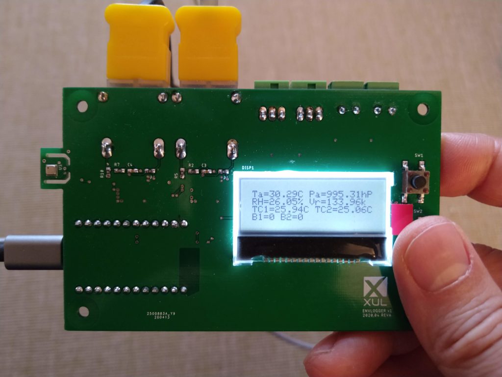
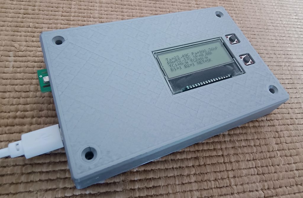
BME680: Ta=30.200001C Pa=995.390000hPa RH=32.077999% VCOR=211.831000kOhm
MCP9601
Either I didn’t spend enough time searching the matrix or once again the crave for reinventing the wheel lurked behind my neck, but I found no ready made libraries.
So I wrote the bare minimum for a test. Writing driver code is always helpful because it forces to read the datasheet thoroughly (it should be mandatory also when integrating the hardware, but..).
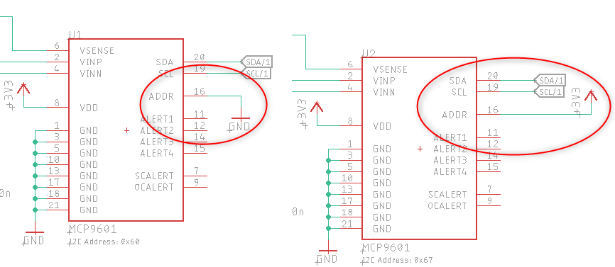
With the minimal set of read/write registers, the first thing to do was to query the devices for their IDs, essentially checking whether both units were operational. The first channel is set on address 0x60 (pin ADDR to GND) and the second on 0x67 (pin ADDR to VDD).
Pulling out data is then relatively easy, after adding the code to convert the short notation of the payload to an actual temperature.
I omit pasting the code here since it can be found on the repo.
Unfinished tasks: the open circuit detection didn’t work as I expected as well as the TH UPDATE bit on the status register. I’ll be back on it as soon as I’ll have more time to spend on the matter.
NHD-C12832A1Z-FSW-FBW-3V3 aka The LCD
This tiny display gave me a lot of headaches. Or better: its documentation did.
Anyway, this LCD is an assembly of a display and a display driver, namely the Sitronix ST7565R, originally conceived for monochrome 65×128 cellular LCD displays.
I started by using the Adafruit ST7565 library (ported for Particle) ending up with just a solid block of highly excited LCD pixels.
Then I had a look at the datasheet provided by Newhaven. Page 9 had what it seemed to be a sample implementation for an initialization routine, where very conveniently no information about the payloads is given. Since page 8 describes the command codes, I translated each payload to its relative command and annotated my code.
The display didn’t give any life sign and I had a limited set of options to understand what was the issue. So I dug a bit more in the ST7565R datasheet and started to feel a bit of frustration because this datasheet couldn’t be specific about the settings required for the display panel in use in the assembly.
So I went back to the Adafruit ported library and modified it to match the settings described in the display’s datasheet (and limiting the number of rows to 32):
The current firmware simply starts by initializing the devices and enters a loop where it polls the devices and prints the relative results to the display.
Having incorporated two buttons opens up a landscape of options in which such device might be able to do everything (logging, control) by just the mean of being configured to do so.
But before spending efforts on such solution, I find that it’d make more sense to implement specific patterns first (such as a simple datalogging setup for starters).
I’ll be sure to write updates on the matter 🙂
Words of wisdom
There are always lessons to be learned, even for such simple integration designs.
What I find relevant to be remembered (yeah, some are part of the baseline requirements, I reckon):
One never stops learning
Employing devices that could achieve high precision requires careful, experienced design
Purpose and usage patterns of a device should be evaluated way before completing the design
Thoroughly reading datasheets is not an option but a must
Achieving perfection is utopian, as well as getting things right at the first attempt. But it’s always good to start from something and have the patience to persevere and iterate
Fail or iteration?
And here the sweet gist: nothing comes out of the world of the ideas without a pinch of effort and unscathed by errors.
Finding the sweet spot between expectations, fuel (determination, budget) and capabilities is and always be an exciting challenge.
Iteration is the key: fail and retry. It’s hard to say when it’s good enough and it’s usually the end user the last judge to this process..
A bitmap representation of a small portion of the linux kernel (I guess v2.something)
Yes, yet another blog.
I’m quite sure I lack the discipline for being a regular writer, but being regular is not my goal.
If there’s something that psyches me out is the fil rouge that binds electronics and programming. I feel equally attracted to both worlds and I believe that their synergy is sublime and very powerful.
I’ve always been a lurker of technical communities and open projects and absorbing information like a sponge has been a constant since I received my first computer, a long, long while ago.
So, to get to the point: I have a couple of ideas that yell from the Hyperuranion to be brutally dragged into existence and I’ll pretend to know how to do it, providing a (hopefully) exhaustive description of my ramblings and tribulations to get there.
So, I hope to give something back to the world in sign of my eternal gratitude.